



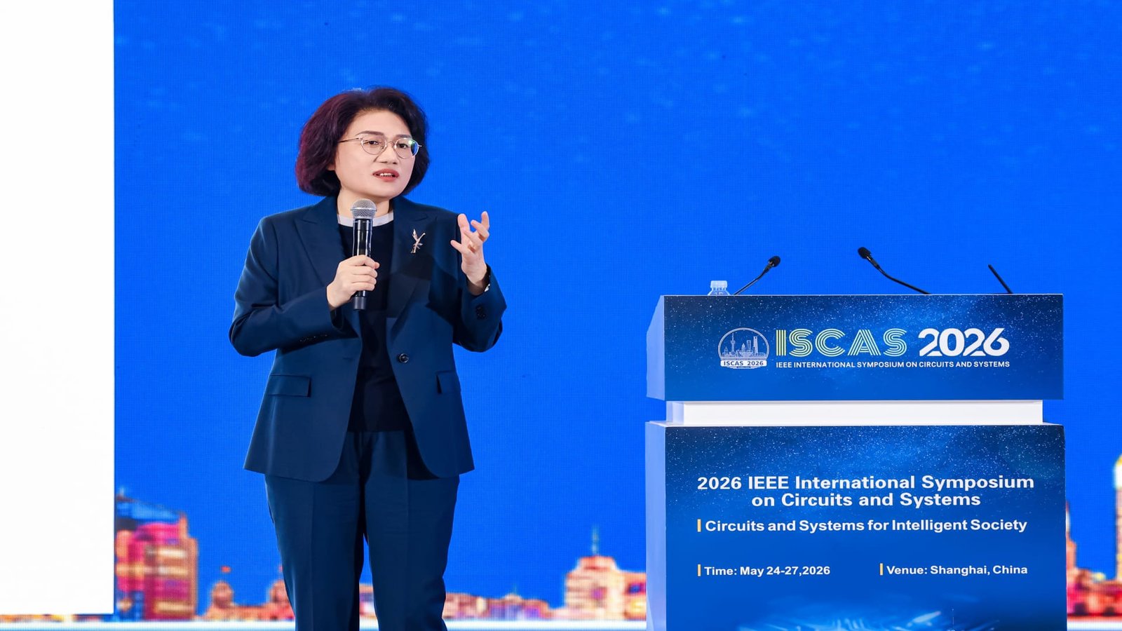
Chinese tech company Huawei announced a new method for semiconductor development despite ongoing U.S. sanctions during a recent conference in Shanghai. The company’s latest engineering approach, named "LogicFolding," aims to enhance the manufacturing of its Kirin smartphone chips, anticipated for release this fall. This innovation coincides with increasing challenges faced by Nvidia in the Chinese market due to U.S. export restrictions.
Huawei’s recent smartphone launch, the Mate 60, features advanced chip technology that has enabled the company to reclaim market share from competitors like Apple. Amid these shifts, Nvidia CEO Jensen Huang acknowledged that the company has effectively ceded the Chinese market to Huawei, indicating that opportunities for selling advanced chips in the region are diminishing.
As Huawei projects that its new chip technology could achieve capabilities similar to 1.4-nanometer process technology by 2031, skepticism persists regarding these claims. Experts warn that while the stacked design may yield efficiency improvements, it does not address the broader challenges related to production processes and performance associated with true 1.4 nm-class manufacturing.
In addition to its engineering approaches, Huawei is striving for greater academic recognition in semiconductor research, recently introducing what it terms the "Law of Tau." This concept aims to optimize chip design and manufacturing processes. However, experts highlight that significant hurdles still exist regarding heat management and scaling production.
Huawei’s advancements may redefine its position in the competitive landscape, but the company remains on a long development path as it seeks to adapt and innovate amidst international trade pressures.
Why this story matters
Key takeaway
Opposing viewpoint